Professional Instrument
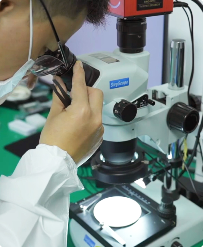
1.Microscope Inspection
Microscope inspection is critical for ensuring the quality and reliability of electronic components. It enables detailed analysis of materials (e.g., semiconductor crystal defects, connector oxidation) , detects microscopic defects like cracks or solder voids , and verifies PCB integrity through plating and layer inspections . High-resolution imaging (e.g., electron or stereo microscopes) allows precise evaluation of solder joints, component alignment, and hidden flaws .
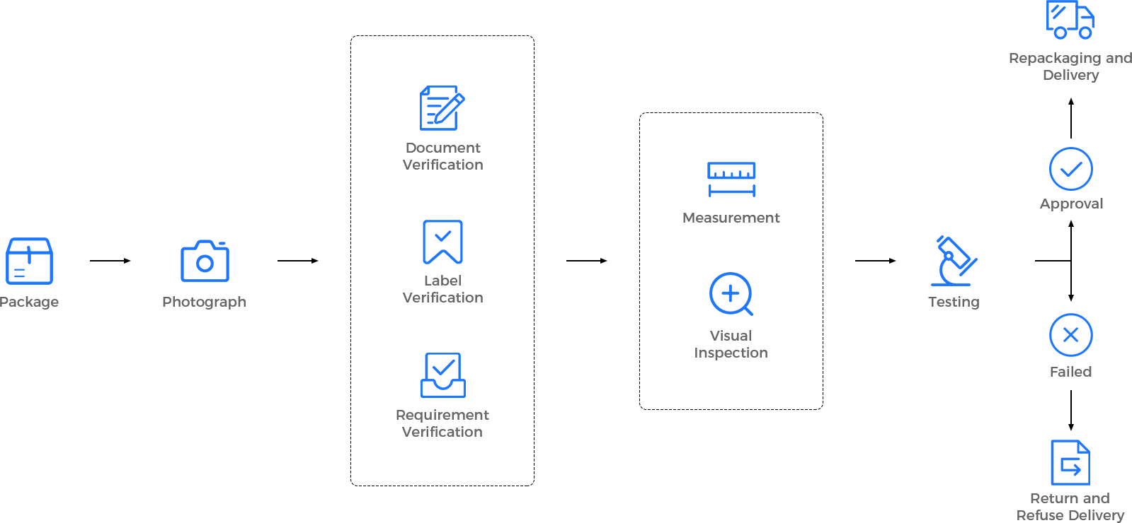
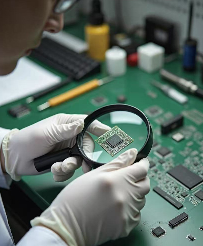
2.Visual Inspection
Conduct visual checks on packaging integrity (no damages, deformations, splicing marks, or leaks) and verify labels for accuracy (product specs, batch numbers, compliance symbols) .
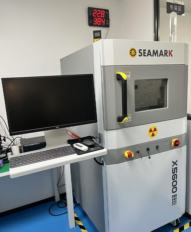
3.X-ray testing
X-ray testing is a non-destructive inspection method widely used in electronics manufacturing to evaluate internal structures and detect hidden defects.
Key Applications:
· Welding & Soldering Inspection.
· Detect voids, cracks, or incomplete connections in BGA, QFN, and SMT joints.
· Verify wire bonding integrity in IC packaging.
· PCB & Component Analysis:
· Identify hidden defects like layer misalignment, short circuits, or broken traces.
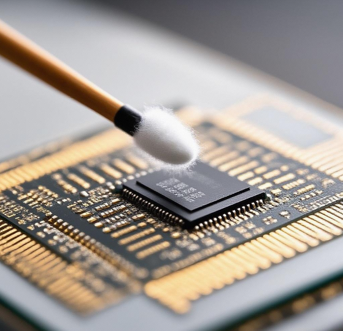
4.Acetone Test
Apply 50%-70% acetone with a cotton swab to wipe the chip marking area. Genuine products show no fading or peeling (laser/ink printing), while refurbished chips exhibit blurred edges or discoloration. Suitable for plastic-encapsulated ICs; avoid excessive acetone corroding pins.
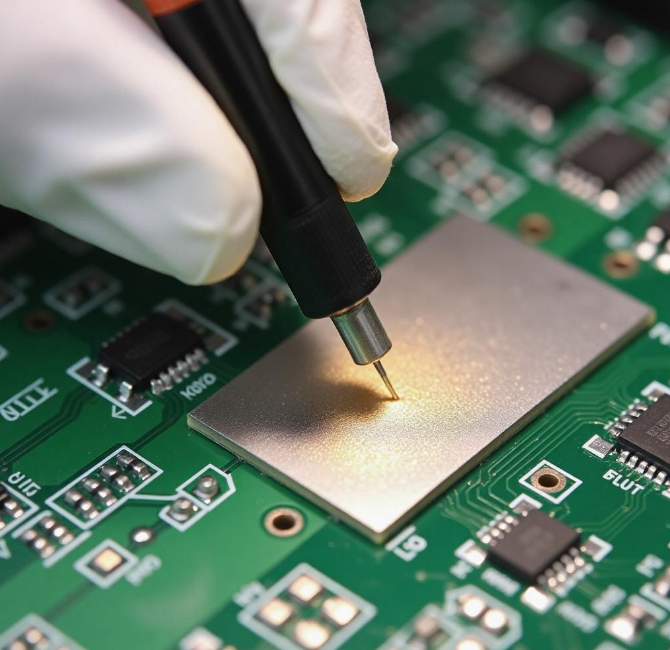
5.Bridge Test (Capacitance/Resistance)
Use a balanced bridge circuit to measure capacitance/resistance. Connect the component to the bridge, adjust variable resistors for balance, and calculate parameters.Achieves ±0.1% accuracy for rapid batch validation.
6.Solder Paste Reflow Test
Print solder paste on substrates and heat to 260°C. Observe spreading, wetting, and void formation. Qualified paste spreads uniformly with no shorts/voids. Validate flux residue via insulation resistance (DC100V) and high-temperature/humidity reliability (40°C/90%RH).